

VCSELs Enable Pocket-Sized Atomic Clocks
Researchers from the Andrew and Erna Viterbi Faculty of Electrical and Computer Engineering together with the staff of the Micro and Nano Fabrication Unit (MNFU) at the Sara and Moshe Zisapel Nanoelectronics Center, have developed unique vertical cavity surface emitting lasers, known as VCSELs, to be used in chip scale atomic clocks. Because of their extremely small size – roughly 1000 of them could fit in a grain of salt – VCSELs are highly energy efficient, a crucial property for the battery-driven, mobile atomic clocks.
Atomic clocks are the most precise man-made machines, and have major impacts on fundamental science and numerous applications, 
including GPS navigation, synchronization of communication and computing systems, as well as defense systems including Iron Dome, to name but a few. The most precise clocks are very large systems, found only in a few national laboratories around the world. Such a clock would miss one second in a time longer than the life of the universe. The so-called cesium fountain clock is somewhat more abundant and is used universally to define one second. Small chip scale atomic clocks were developed to enable very small, inexpensive, and mobile, yet accurate, time measurement. These battery-driven clocks would lose one second in 10,000 years. At its heart is a special VCSEL that was recently developed by the Technion.
This particular VCSEL has many characteristics that are difficult to implement, including very high accuracy of their light emission color, shape, and polarization, as well as the ability to operate at extremely high temperatures. The Technion successfully developed such VCSELs, that even outperform the best commercially available competitors.
The VCSEL development project was part of an industry-academia consortium initiated by the Israel Innovation Authority (IIA).  It includes, in addition to the Technion, commercial companies such as NVIDIA, SCD, Civan, Accubeat, and PCB, and the Hebrew University of Jerusalem. The roots for establishing the VCSEL development lie in the vision of the IIA for the significance of VCSELs to the Israeli industry, and in a long-term collaboration between the Technion and the Israeli branch of NVIDIA (formally Mellanox). However, the most important contribution to the success is the Technion itself whose scientific and technological excellence enabled this major breakthrough.
The Technion researchers within the consortium include Professors Meir Orenstein, Gadi Eisenstein, and Mordechai (Moti) Segev from the Andrew and Erna Viterbi Faculty of Electrical and Computer Engineering. 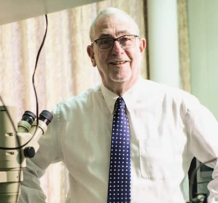 Professor Eisenstein, the director of the Russell Berrie Nanotechnology Institute and the head of the MNFU explains that the key figure in this project is Prof. Orenstein, a well-known expert in VCSEL technology. He designed the material structure and the device processing procedures and supervised their fabrication in the MNFU. The excellent MNFU staff, led by Director Aya Cohen, showed unequivocal capability in developing state-of-the-art devices that rival those fabricated by commercial manufacturers.
The consortium is developing other types of VCSELs, in addition to those for atomic clocks. 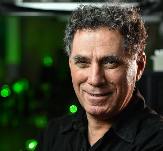
NVIDIA leads a working group on high speed VCSELs for data communication and SCD is responsible for high power VCSEL arrays. The latter has two parts. Prof. Orenstein is developing one based on his invention of a coherent VCSEL array, a light source composed of hundreds of VCSELs working in conjunction to produce a high brightness light beam. The second solution is an array of topological VCSELs, which are unique in that they are immune to external disturbances, developed by Distinguished Prof. Mordechai (Moti) Segev – the inventor of the topological laser.
The field of microelectronics was brought to the Technion in the early 1970s by Professor Izhak Kidron. Semiconductor device fabrication started after the 1973 war when the Technion took it upon itself to develop a solution to a crucial deficiency: infrared detection systems that no country was willing to supply Israel with. The successful development of those devices marked the starting point of microelectronics in Israel. Micro – and later nano – electronics activities at the Technion have continuously grown ever since and are considered “the cradle of the flourishing Israeli electronics industry.”
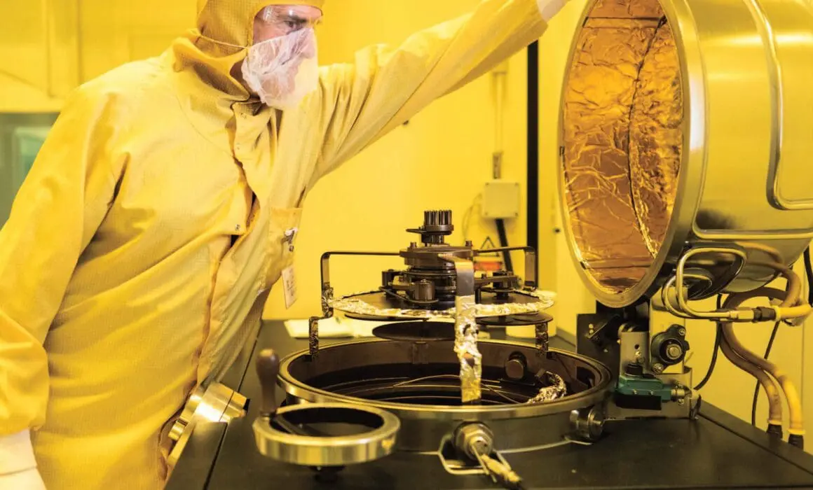
The present Technion fabrication facility is the MNFU, which boasts 700 m2 of cleanrooms, making it the largest center of its kind in any Israeli university. 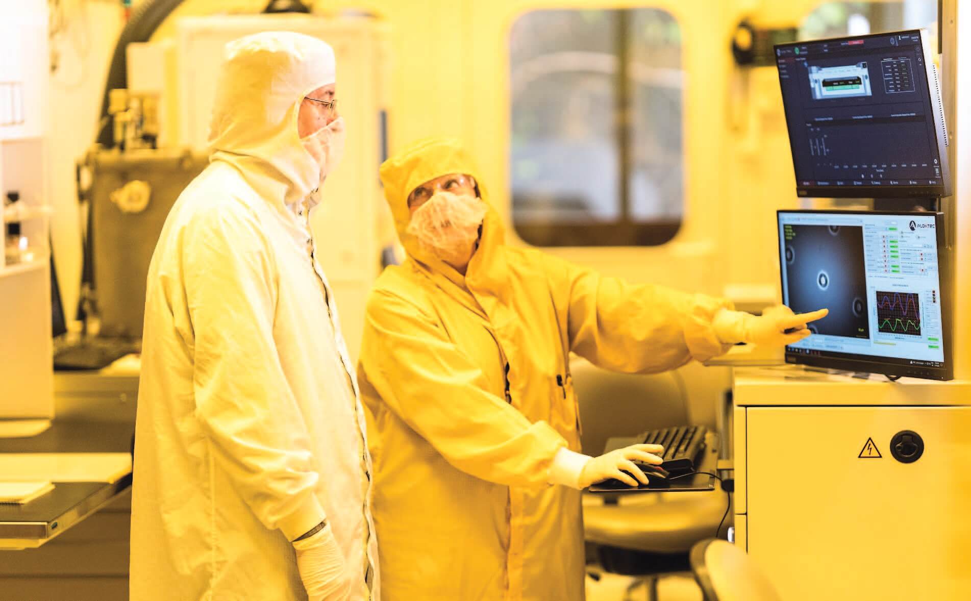
It is a shared research and development facility supporting numerous academic researchers, graduate students, and industrial researchers. The Center offers a complete set of micro- and nano-fabrication tools, as well as process and prototype developments led by its excellent engineering staff. This combines the best of two worlds: academic expertise, flexibility, and creativity together with the high-performance standards required by the industry.
More Protecting Our Planet stories


Breathing New Life into Hydrogen Fuel Cells